
Custom CNC Machined PEEK U-Shaped Wafer Positioning Fixture for Semiconductor Automation Equipment
Description
Product Introduction
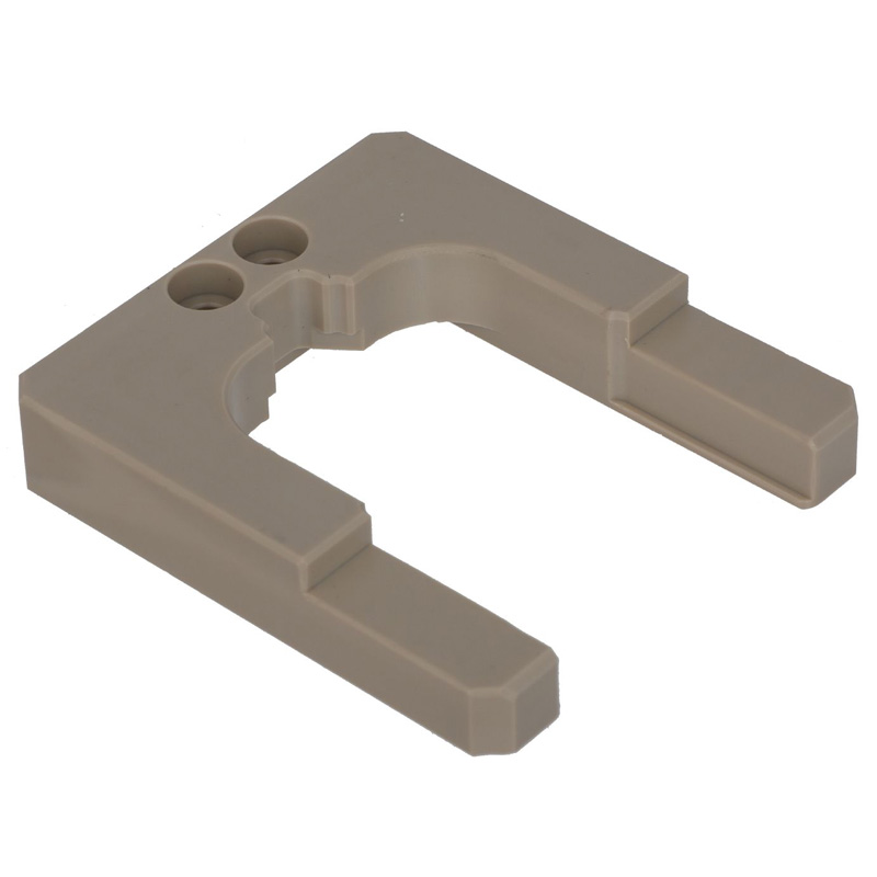
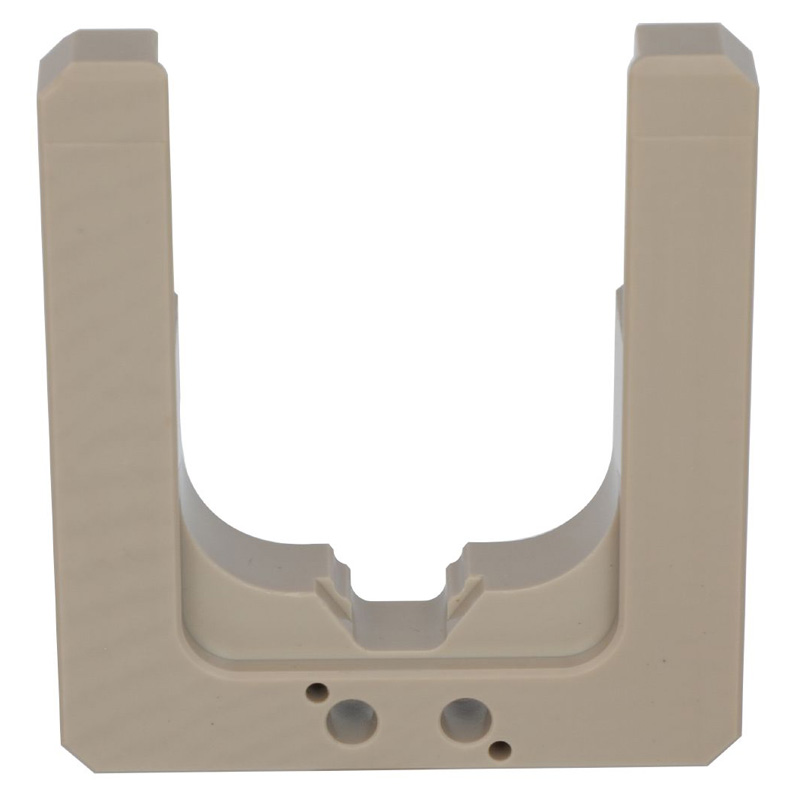
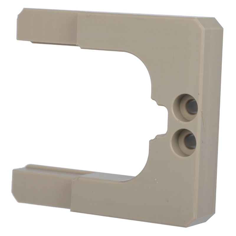
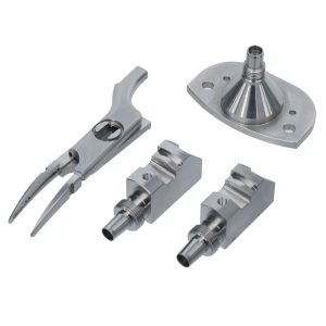
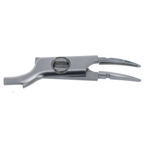
This custom CNC machined PEEK U-Shaped fixture is engineered specifically for the delicate handling, positioning, and nesting of cylindrical or thin-plate precision components. Featuring a U-shaped open structure with internal locating notches, dual precision pin holes, and two counterbored mounting holes, this fixture ensures accurate, vibration-free, and scratch-free placement of workpieces.
While it is the industry standard for semiconductor wafer gripping and positioning (as a Wafer Nest) due to PEEK’s ultra-low outgassing properties, this versatile automation component is equally ideal for medical catheter positioning, sensor housing fixation, and high-end optical lens assembly.
CNC Machining Services & Specifications Table
(Structured for Google Rich Snippet/Knowledge Graph optimization)
| Parameter | Specification / Capability |
|---|---|
| Machining Process | 3-Axis / 4-Axis / 5-Axis CNC Milling, Drilling, Counterboring, Chamfering |
| Raw Material | PEEK (Virgin, Unfilled / 450G / 30% Glass-filled variants available) |
| Standard Tolerance | ±0.01 mm (H7, G6 fits achievable for pin holes) |
| Premium Precision | ±0.005 mm (Upon request, for semiconductor high-cleanliness requirements) |
| Surface Finish | High-speed machining finish (Ra 0.8 – 1.6 μm), Deburred edges (specifically for U-shape arms) |
| Cleanliness Level | Class 100 / Class 1000 Cleanroom compatible (Ultrasonic cleaning + Vacuum packaging) |
| Minimum Order (MOQ) | 1 Piece (Prototype to mass production) |
| Lead Time | 3 – 5 business days for prototyping; 7 – 15 days for mass production |
| Inspection Equipment | CMM (Coordinate Measuring Machine), 2.5D Vision Measuring System, Micrometers |
| Quality System | ISO 9001:2015, ISO 13485 (Medical) certified upon request |
Application Scenarios (Where is it used?)
Thanks to its U-shaped open nest design, this part serves critical functions across three high-end sectors:
-
Semiconductor & Wafer Handling (Primary): Used as a Wafer Positioning Nest / End Effector Gripper to hold 4-inch, 6-inch, 8-inch, or 12-inch silicon wafers during transport, etching, or inspection inside vacuum chambers.
-
Medical Device Automation: Utilized as a Catheter Syringe Clamping Jig or Sensor Probe Fixation Bracket in automated IV pumps, diagnostic analyzers, and assembly lines for medical tubes.
-
3C & Optical Precision Assembly: Used as an Assembly Alignment Block to temporarily secure cylindrical motor housings, lens barrels, and connectors before soldering or press-fitting.
Material Analysis: Why PEEK over Metal or POM?
The choice of PEEK (Polyether Ether Ketone) is not accidental; it is a technical mandate for high-end automated equipment.
-
Ultra-Low Outgassing & Cleanliness: Unlike POM (Delrin) or Nylon, PEEK does not release volatile gases or particles in vacuum environments, making it essential for semiconductor cleanrooms (Class 100).
-
Non-Abrasive & Scratch-Free: It will never scratch delicate silicon wafers, optical lenses, or medical coatings, whereas aluminum or stainless steel jaws cause micro-scratches that lead to defect rates.
-
High Temperature & Chemical Resistance: Resistant to sustained 260°C (500°F) heat and harsh chemical cleaning agents (ACID, IPA) used in semiconductor and pharmaceutical cleaning processes.
-
Excellent Mechanical Strength: Offers high stiffness and creep resistance even at elevated temperatures, ensuring the U-shaped arms do not bend or fatigue over millions of robotic actuation cycles.
Tolerance Capabilities
Achieving extreme precision on plastic materials is harder than on metals. Our facility guarantees:
-
Pin-hole positioning: Down to ±0.005mm to ensure absolute mating with the automation base plate without any play.
-
U-Shape Arm Parallelism: Down to 0.02mm over a 100mm span, preventing wafer tilting or glass breakage.
-
Inner Arc Radius: Customizable to exact radii (e.g., R50, R100, R150) with tolerance ±0.01mm to perfectly wrap around cylindrical workpieces.
Manufacturing Difficulties (Why choose a pro?)
Machining PEEK into a U-shape is technically challenging. Our engineers must overcome:
-
Thermal Deformation during Machining: PEEK has a high coefficient of thermal expansion. If the coolant is not properly managed, the long U-shaped arms will warp or vibrate during milling (chatter marks).
-
Stress Relief: PEEK rods carry internal residual stress. We implement a pre-machining annealing treatment (Stress Relieving) to unlock internal stress, ensuring the final U-shape remains straight after unclamping from the CNC fixture.
-
Deburring the Inner Cutouts: The inner groove and locating notches have sharp edges when machined. We utilize manual ceramic deburring + CBN polishing to achieve a mirror-smooth inner wall (Ra < 0.4 μm), completely eliminating burrs that might shed particles.
Frequently Asked Questions (FAQ)
Q1: Can this U-shaped fixture be autoclaved for medical use?
A: Yes, PEEK is fully steam autoclavable (up to 134°C) and compatible with EtO sterilization, making it perfect for medical automation applications.
Q2: How do the two smaller holes function on the base?
A: Those are precision dowel pin holes. In automation engineering, they serve as a mechanical “foolproof” positioning mechanism. They ensure the fixture aligns perfectly with the pneumatic slide or robotic arm every single time, maintaining repeatability within 0.01mm.
Q3: What is the difference between CNC machining and injection molding for this part?
A: This part is exclusively CNC machined. Semiconductors and medical instruments require high-performance virgin PEEK without flow lines or weld marks. CNC allows us to make small-batch customizations (e.g., changing inner diameter for a different wafer size) without expensive injection molds.
Q4: Is this PEEK electrically conductive?
A: Standard PEEK is an excellent electrical insulator. If anti-static (ESD) properties are required for your semiconductor environment, we can infuse it with carbon fiber, or recommend a black anti-static PEEK alternative.
Real-World Case Study (Actual Case)
Client: A leading Semiconductor Equipment Manufacturer in the USA.
Challenge: The client was using standard aluminum alloy wafer grippers. The metal particles generated from friction were causing short circuits on the chips. They needed a non-metallic, heat-resistant, U-shaped positioning fixture with precise alignment holes, specifically for 12-inch wafers in a 200°C rapid thermal processing (RTP) machine.
Our Solution:
We reverse-engineered their design and recommended Virgin Natural PEEK (unfilled). Our CNC team machined the U-shaped fixture on a 5-axis machine to guarantee a perfectly smooth inner arc. We added stress-relieving steps to ensure the two arms remained perfectly parallel even after high-temperature cycles.
Result: The PEEK fixture reduced the particle contamination yield loss by 98% and successfully withstood over 5 million robotic pick-and-place cycles without cracking or warping, increasing the client’s semiconductor fab production efficiency.
Additional information
| material |
|---|


Reviews
There are no reviews yet.