
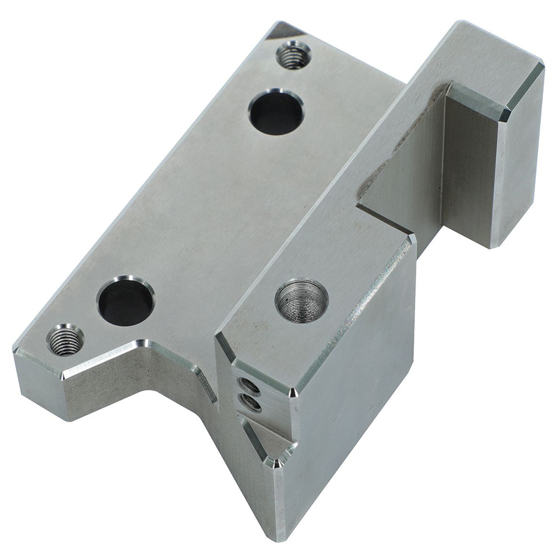
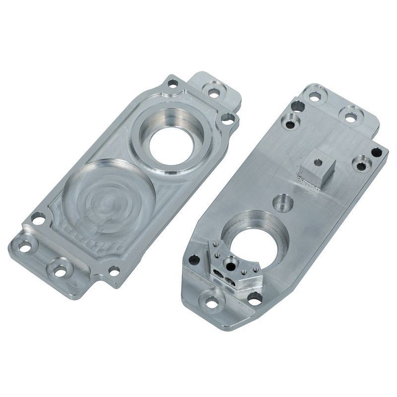
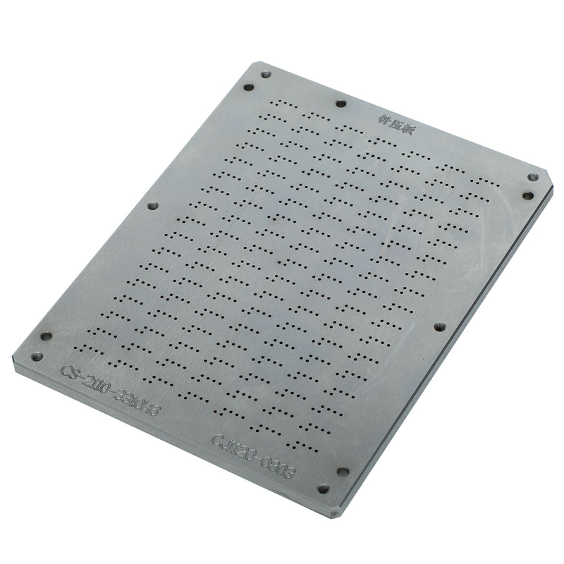
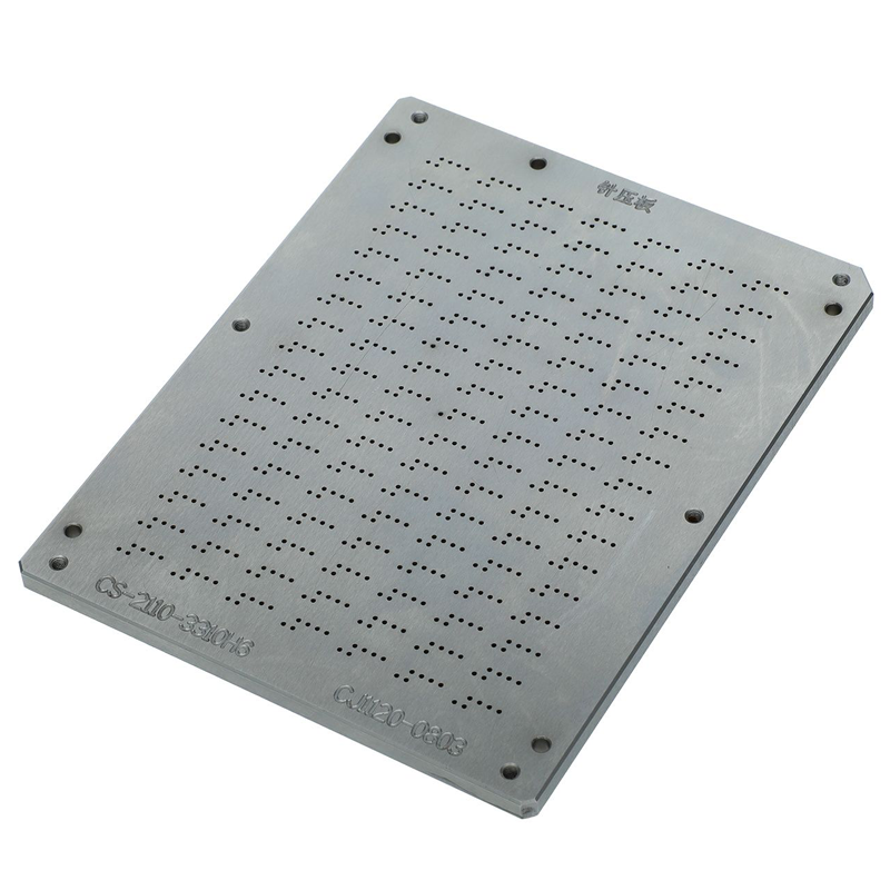
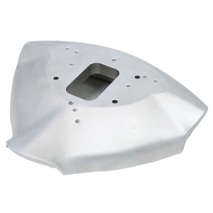
Custom CNC Machined SKD11 Tool Steel Probe Guide Plate for PCB ICT Test Fixtures
Description
Product Overview
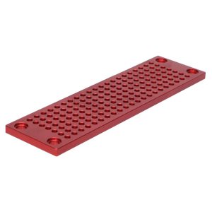
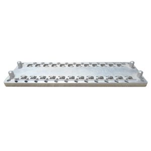
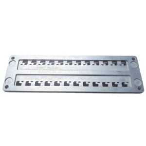
The Custom CNC Machined SKD11 Tool Steel Probe Guide Plate is a precision-engineered core component designed for In-Circuit Test (ICT) and bed-of-nails test fixtures in PCB manufacturing. As one of our core precision CNC Plate solutions, it acts as the critical interface between the test fixture and the printed circuit board, ensuring accurate probe alignment, consistent electrical contact, and reliable test results across high-volume production runs.
Manufactured from premium SKD11 cold-work tool steel — the JIS equivalent to AISI D2 and DIN 1.2379 — this probe guide plate delivers exceptional wear resistance, dimensional stability, and longevity that far outperforms conventional aluminum or plastic alternatives. Each plate is custom CNC machined from customer-provided Gerber files or probe coordinate data, with precision-drilled holes that guide spring-loaded probes to their designated test points with micron-level accuracy.
Whether you are testing high-density PCBA for consumer electronics, automotive modules, or telecommunications equipment, our SKD11 probe guide plates provide the durability and precision required for thousands of reliable test cycles.
Material Analysis: SKD11 Tool Steel
SKD11 is a high-carbon, high-chromium cold-work tool steel renowned for its outstanding hardness, wear resistance, and dimensional stability. Under the Japanese Industrial Standards (JIS) classification, SKD11 is the preferred material for high-precision tooling applications requiring long service life under repetitive loading conditions.
Chemical Composition (JIS G4404 Standard)
| Element | Typical Range (%) | Primary Function |
|---|---|---|
| Carbon (C) | 1.40 – 1.60 | Forms carbides; contributes to hardness and wear resistance |
| Chromium (Cr) | 11.00 – 13.00 | Enhances hardenability, wear resistance, and corrosion resistance |
| Molybdenum (Mo) | 0.80 – 1.40 | Increases toughness and supports secondary hardening |
| Vanadium (V) | 0.15 – 0.50 | Refines grain size; stabilizes carbides; improves wear resistance |
| Silicon (Si) | ≤ 0.40 – 0.50 | Deoxidizer; contributes to strength |
| Manganese (Mn) | ≤ 0.50 – 0.60 | Supports hardenability; reduces cracking tendency |
| Phosphorus (P) | ≤ 0.030 | Impurity control; reduces brittleness |
| Sulfur (S) | ≤ 0.030 | Impurity control |
Key Mechanical Properties
-
Hardness: After proper heat treatment, SKD11 achieves 58–62 HRC, allowing it to withstand immense pressures without deformation or dulling
-
Wear Resistance: The high volume of hard chromium carbides in the steel matrix provides outstanding resistance to abrasive and adhesive wear
-
Compressive Strength: Exceptional resistance to crushing under high loads
-
Toughness: Sufficient for cold-work applications, resisting chipping and cracking under typical impact loads
-
Dimensional Stability: As an air-hardening steel, SKD11 experiences minimal distortion during quenching — critical for maintaining tight tolerances in complex guide plates
-
Density: 7.7 g/cm³
-
Equivalent Standards: AISI D2, DIN 1.2379, EN X153CrMoV12
Why SKD11 for Probe Guide Plates?
| Requirement | SKD11 Advantage |
|---|---|
| Repeated probe insertion/retraction | Exceptional wear resistance extends service life |
| High spring forces (up to 500+ lbs total) | High compressive strength prevents deformation |
| Tight hole positional tolerances | Excellent dimensional stability after heat treatment |
| Thousands of test cycles | Maintains sharp edges and precision over prolonged use |
| Contact with PCB surfaces | Non-galling; maintains surface finish integrity |
Application Scenarios
Primary Applications
1. In-Circuit Test (ICT) Fixtures
The probe guide plate serves as the precision-drilled plate that holds one spring-loaded probe per test point, wired back to the tester’s channels. The board is pulled down onto the probes via vacuum or mechanical press, enabling simultaneous electrical access to every net on the PCB.
2. Functional Circuit Test (FCT) Fixtures
For functional testing where PCBA must be validated under operational conditions, SKD11 guide plates provide the mechanical stability required for consistent signal integrity.
3. Bed-of-Nails Test Systems
As a core component of “bed-of-nails” test systems, the guide plate ensures that hundreds or thousands of spring-loaded probes make simultaneous contact with their designated test points.
4. Semiconductor Test Handlers
For high-wear test pins and jigs in semiconductor packaging and final test applications, SKD11 components are heat-treated to HRC 60+ and ground to sub-micron tolerances.
Industry Sectors
| Sector | Application |
|---|---|
| Consumer Electronics | Smartphone, tablet, and wearable PCBA testing |
| Automotive | ECU, sensor, and infotainment module ICT |
| Telecommunications | Network equipment and base station board testing |
| Medical Devices | High-reliability PCBA for diagnostic equipment |
| Industrial Automation | Control board and power module verification |
| Aerospace & Defense | Mission-critical PCB testing with zero-defect requirements |
Typical Fixture Configuration
A complete ICT test fixture consists of:
-
Base plate: Supports the overall structure
-
Probe guide plate (this product): Houses the test pins with precision-drilled holes
-
Guide pins: Ensure accurate registration between the fixture and PCB
-
Spring-loaded probes: Provide electrical contact to PCB test points.
CNC Machining Service Parameters
Our precision CNC machining capabilities for SKD11 tool steel probe guide plates are summarized below:
General Specifications
| Parameter | Specification |
|---|---|
| Material | SKD11 tool steel (JIS G4404) — equivalent to AISI D2 / DIN 1.2379 |
| Material Condition | Spheroidized annealed (~210–255 HB) for optimal machinability |
| Heat Treatment | Vacuum heat treatment to 58–62 HRC |
| Post-Heat Treatment | Precision grinding to final dimensions |
| Surface Finish | Ra 0.2 – 0.8 μm after precision grinding |
Dimensional Capabilities
| Parameter | Capability |
|---|---|
| Dimensional Tolerance | ±0.005 mm to ±0.01 mm |
| Hole Positional Tolerance | ±0.005 mm |
| Flatness | ≤ 0.01 mm per 100 mm |
| Parallelism | ≤ 0.01 mm |
| Minimum Hole Diameter | ≤ φ0.1 mm (micro-drilling capability) |
| Surface Roughness (Ra) | < 0.2 μm (precision ground) |
| Maximum Plate Size | Custom per customer requirements |
Process Capabilities
| Process | Description |
|---|---|
| CNC Milling | 3-axis, 4-axis, and 5-axis machining for complex geometries |
| Micro-Hole Drilling | ≤ φ0.1 mm with ±0.005 mm positional tolerance |
| Wire EDM | For ultra-fine slots, edge profiling, and sharp corners |
| Precision Grinding | Flatness < 0.005 mm and Ra ≤ 0.1 μm |
| Vacuum Heat Treatment | Controlled process ensuring minimal distortion |
Inspection & Quality Control
| Equipment | Application |
|---|---|
| CMM (Coordinate Measuring Machine) | Dimensional measurement and geometric tolerance verification |
| Nikon Vision System | Micro-feature inspection |
| Height Gauge | Planarity and parallelism measurement |
| Surface Profiler | Surface roughness and burr inspection |
| Hardness Tester | Verification of heat treatment results |
Recommended Cutting Parameters (Reference)
For SKD11 machining, optimal parameters vary based on hardness state:
| Parameter | Annealed (~210 HB) | Pre-hardened (~45 HRC) | Hardened (~58–62 HRC) |
|---|---|---|---|
| Cutting Speed (Vc) | 130–180 m/min | 80–130 m/min | 40–80 m/min |
| Feed per Tooth (fz) | 0.08–0.15 mm/tooth | 0.05–0.10 mm/tooth | 0.03–0.08 mm/tooth |
| Depth of Cut | 0.5–2.0 mm | 0.3–1.0 mm | 0.1–0.5 mm |
| Tool Material | Carbide (uncoated) | Coated carbide (TiAlN/TiCN) | Coated carbide / CBN |
| Coolant | Flood coolant | MQL or flood coolant | MQL or air cooling |
Note: Optimal parameters for SKD11 milling have been established at Vc=130 m/min, fz=0.12 mm/rev, and ap=1.0 mm for achieving surface quality comparable to fine grinding (Ra=0.642 μm).
Tolerance Capabilities
Our probe guide plates are manufactured to the tightest tolerances required for high-density ICT fixtures:
Standard Tolerances
| Tolerance Type | Capability | Application |
|---|---|---|
| Dimensional Tolerance | ±0.01 mm (standard); ±0.005 mm (precision) | Overall plate dimensions |
| Hole Diameter Tolerance | H7 tolerance class | Probe receptacle holes |
| Hole Positional Tolerance | ±0.005 mm | Probe grid alignment |
| Flatness | ≤ 0.01 mm per 100 mm | Contact surface planarity |
| Parallelism | ≤ 0.01 mm | Top-bottom surface alignment |
| Perpendicularity | ≤ 0.01 mm | Hole-to-surface perpendicularity |
| Surface Finish | Ra 0.2 – 0.8 μm | Probe sliding surfaces |
Achieving ±0.005 mm Precision
To achieve the ±0.005 mm tolerance required for high-density probe plates, our manufacturing process incorporates:
-
High-rigidity CNC machines with thermal compensation
-
Precision tooling with carbide or PVD-coated cutting tools
-
Controlled cutting parameters optimized for SKD11
-
Stress-relief annealing between rough and finish machining
-
Vacuum heat treatment to minimize distortion
-
Precision grinding as a finish operation
-
100% CMM inspection
Why Tight Tolerances Matter for ICT Fixtures
In high-density PCB testing, test pads can be as small as 0.5 mm diameter with probe spacing below 0.028 inches (0.71 mm). Even a positional deviation of 0.01 mm can cause a probe to miss its target or contact adjacent pads, resulting in false failures or shorts. Our ±0.005 mm hole positional tolerance ensures reliable contact even with the smallest test points.
Furthermore, all test points must maintain coplanarity within ±0.05 mm; otherwise, some probes may fail to make contact. Our flatness capability of ≤ 0.01 mm per 100 mm ensures that the entire probe array contacts the PCB uniformly.
Manufacturing Challenges
Machining SKD11 tool steel into high-precision probe guide plates presents several significant challenges that require specialized expertise:
1. Material Hardness and Tool Wear
Challenge: SKD11’s high hardness and chromium-carbide content cause accelerated cutting tool wear, high cutting temperatures, and compromised surface finish. Machining SKD11 after heat treatment presents even greater challenges due to high cutting forces and elevated temperatures.
Solution:
-
Use carbide or PVD-coated (TiAlN/TiCN) cutting tools
-
Optimize cutting parameters (speed, feed, depth of cut)
-
Implement MQL (Minimum Quantity Lubrication) or flood coolant
-
Employ high-rigidity machine tools and tool holders
2. Heat Generation and Thermal Deformation
Challenge: SKD11 has poor thermal conductivity, and local high temperatures during CNC machining can affect tool life and cause thermal deformation of the workpiece.
Solution:
-
Use effective cooling methods to counteract heat generation
-
Allow for cooling periods between roughing and finishing passes
-
Apply stress-relief annealing after heavy machining
3. Material Distortion
Challenge: SKD11 is sensitive to heat and internal stresses, which can cause material distortion during CNC machining. Vacuum heat treatment of SKD11 can also cause specific distortion patterns depending on material thickness.
Solution:
-
Machine in annealed condition before heat treatment
-
Apply stress-relieving cycle at 650–675°C (1200–1250°F)
-
Allow machining stock for post-heat-treatment grinding
-
Use wire EDM for final features on hardened material
4. Surface Finish Quality
Challenge: The hardness of SKD11 poses challenges in achieving a smooth surface finish, often requiring additional finishing operations.
Solution:
-
Employ precision grinding as a finish operation
-
Use fine-grit grinding wheels with appropriate bonds
-
Implement lapping for mirror finishes (Ra ≤ 0.1 μm)
-
Optimize milling parameters to achieve surface quality comparable to grinding (Ra=0.642 μm)
5. Micro-Hole Drilling
Challenge: Probe guide plates for high-density ICT fixtures require hundreds or thousands of micro-holes (< φ0.2 mm) with ±0.005 mm positional accuracy.
Solution:
-
Specialized micro-drilling CNC equipment
-
High-speed spindles with minimal runout
-
Precision tool presetting and tool length measurement
-
Rigorous in-process inspection
6. Heat Treatment Control
Challenge: Achieving consistent 58–62 HRC hardness while minimizing distortion requires precise heat treatment control.
Solution:
-
Vacuum heat treatment with controlled heating and cooling rates
-
Air-hardening process that minimizes distortion
-
Post-heat-treatment tempering for toughness optimization
-
Hardness verification on each production batch
Frequently Asked Questions (FAQ)
Q1: What is the difference between SKD11 and AISI D2?
SKD11 is the Japanese JIS equivalent to AISI D2 and DIN 1.2379. While they belong to the same steel grade, SKD11 typically offers slightly higher impact toughness due to stricter quality control and electroslag remelting (ESR) processes that minimize impurities such as sulfur and phosphorus.
Q2: Why use SKD11 instead of aluminum or FR-4 for probe guide plates?
Aluminum and FR-4 are common materials for lower-volume or less-demanding applications. However, SKD11 offers:
-
Superior wear resistance for high-volume production (thousands of cycles)
-
Higher compressive strength to withstand the 500+ lbs of spring force in dense ICT fixtures
-
Better dimensional stability over temperature cycles
-
Longer service life — up to 10× longer than aluminum alternatives
Q3: What hardness range can SKD11 achieve after heat treatment?
SKD11 achieves 58–62 HRC after proper quenching and tempering. The material is typically supplied in a spheroidized annealed condition (~210–255 HB) for optimal machinability, then vacuum heat-treated to final hardness.
Q4: What is the minimum hole size you can machine in SKD11?
We can machine holes as small as φ0.1 mm with ±0.005 mm positional tolerance using specialized micro-drilling equipment. For larger production volumes, hole diameters down to φ0.2 mm are standard.
Q5: How do you ensure hole positional accuracy across hundreds of holes?
We use:
-
Precision CNC machines with thermal compensation
-
High-rigidity tool holders and carbide tooling
-
Optimized cutting parameters for SKD11
-
In-process inspection and 100% CMM verification
-
Post-heat-treatment precision grinding
Q6: What is the typical lead time for custom SKD11 probe guide plates?
Lead times vary based on complexity, hole count, and quantity. Typical ranges:
-
Prototype (1–5 pcs): 5–10 business days
-
Small batch (5–50 pcs): 10–15 business days
-
Production (50+ pcs): 15–25 business days
Rapid prototyping (under 7 days) is available for urgent requirements.
Q7: Do you offer heat treatment services?
Yes, we provide in-house vacuum heat treatment with precise temperature control to achieve 58–62 HRC. Heat treatment is performed after rough machining and before final precision grinding to minimize distortion.
Q8: What inspection reports do you provide?
We provide comprehensive quality documentation including:
-
CMM inspection reports with dimensional measurements
-
Hardness test certificates
-
Surface roughness measurement reports
-
First Article Inspection (FAI) reports
-
PPAP documentation upon request
Q9: Can you machine probe guide plates from customer-provided Gerber files?
Yes. We can extract probe coordinates directly from Gerber files or from a defined list of interface probe points. We accept:
-
Gerber files (RS-274X)
-
DXF/DWG drawings
-
STEP/IGES 3D models
-
Excel/CSV coordinate lists
Q10: How do I maintain and clean SKD11 probe guide plates?
-
Regular cleaning: Remove debris with isopropyl alcohol and lint-free wipes
-
Inspection: Check for probe hole wear or damage after each production shift
-
Storage: Apply anti-rust oil and store in a dry environment
-
Replacement: Replace when hole wear exceeds 0.01 mm from original diameter
Q11: Is SKD11 corrosion-resistant?
While SKD11 offers better corrosion resistance than lower-chromium steels, it is not stainless steel. Proper maintenance and anti-rust protection are recommended, especially in humid environments. For applications requiring higher corrosion resistance, consider plated or coated options.
Q12: What is the maximum plate size you can machine?
Maximum plate size depends on our CNC machine capabilities. Please contact us with your specific size requirements for a custom quote. Large plates may require specialized fixturing to maintain flatness and positional accuracy.
Q13: Do you offer surface treatments or coatings?
Yes, we offer additional services including:
-
Nickel plating
-
Gold plating
-
Black oxide coating
-
Anti-rust treatment
Q14: What is the difference between machining SKD11 in annealed vs. hardened condition?
Annealed condition (~210 HB): Easier to machine, allows higher cutting speeds and feeds, but requires post-machining heat treatment.
Hardened condition (58–62 HRC): Much more difficult to machine, requires specialized tooling and lower cutting parameters, but eliminates heat-treatment distortion risk.
Our standard process machines in the annealed condition, heat treats, then performs final precision grinding.
Q15: Can SKD11 be welded or repaired?
SKD11 is not recommended for welding due to its high carbon and chromium content, which can cause cracking. Worn probe guide plates should be replaced rather than repaired to ensure test reliability.
Why Choose Our SKD11 Probe Guide Plates?
| Feature | Benefit |
|---|---|
| Premium SKD11 material | 10× longer service life than aluminum alternatives |
| ±0.005 mm positional tolerance | Reliable contact even with smallest test pads |
| Vacuum heat treatment | Consistent 58–62 HRC with minimal distortion |
| 100% CMM inspection | Guaranteed dimensional accuracy |
| Custom from Gerber files | Seamless integration with your fixture design |
| Rapid prototyping | 7-day turnaround for urgent requirements |
| Competitive pricing | High-quality at cost-effective rates |
Contact us today with your Gerber files or drawings for a customized quote on your SKD11 probe guide plate requirements.
Additional information
| material |
|---|

Reviews
There are no reviews yet.