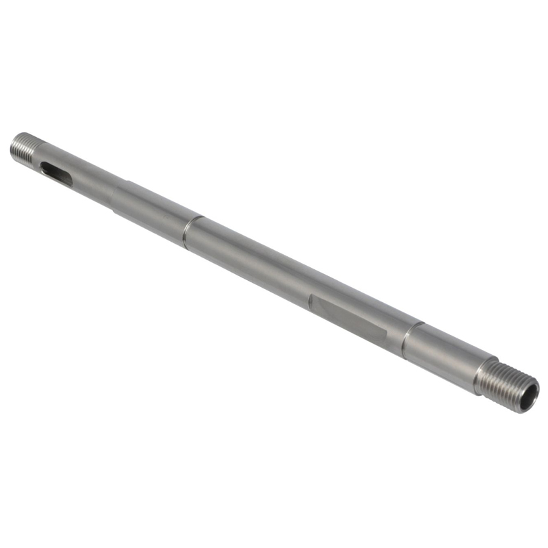
OEM ODM Semiconductor Package Substrate CNC Precision Machining Custom Size for IC Chip
Description
High-Precision Semiconductor Package Substrate | Precision CNC Machining China for Semiconductor Packaging
Introducing our high-performance Semiconductor Package Substrate, engineered to deliver exceptional precision and reliability for advanced IC chip packaging processes. Backed by our state-of-the-art CNC machining China capabilities, we combine cost-effective manufacturing with industry-leading accuracy to meet the stringent demands of semiconductor production.
Core Manufacturing Advantages
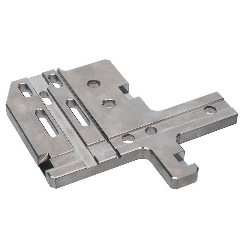
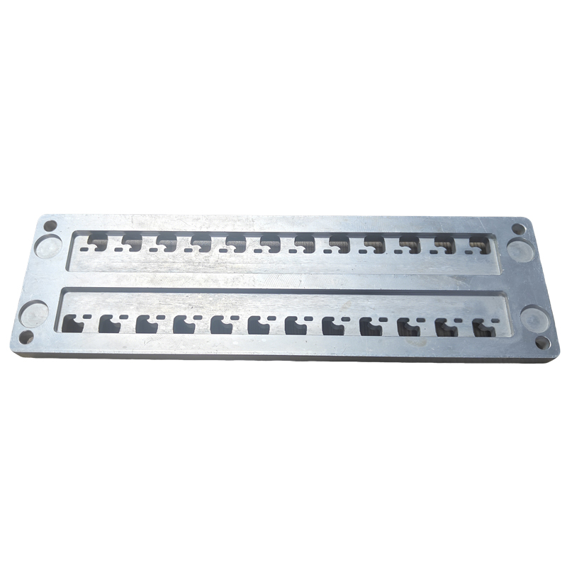
Our substrate is crafted from 6061-T6 aluminum alloy—a fixture-grade material optimized for high-speed CNC milling. Leveraging CNC machining China expertise, our 3-axis precision machining centers achieve tight tolerances: slot width ±0.02mm, hole position accuracy ≤0.01mm, and surface roughness Ra ≤1.6μm on critical working surfaces. The full production flow—from milling and precision boring to deburring and laser marking—is completed in-house within ISO 13485 certified cleanrooms, ensuring zero contamination and consistent quality.
Key Performance Features
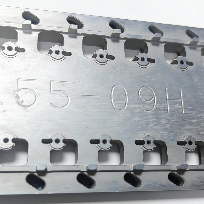
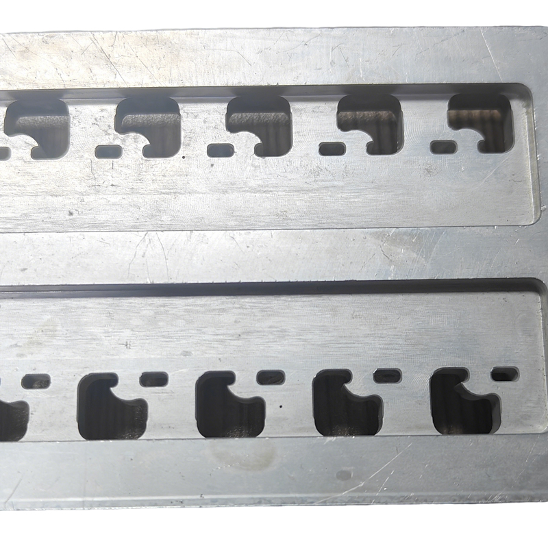
- Precision Alignment: Locating pin holes (φ8H7) and datum pins (φ6mm) ensure stable positioning during die attach and wire bonding processes, eliminating alignment errors.
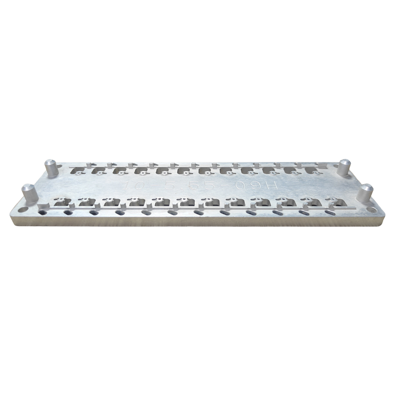
- Traceability: Custom fiber laser marking (e.g., 10-5.555-09H) is applied post-CNC machining, providing permanent, wear-resistant part identification for production tracking.
- Cleanroom Compliance: Ultrasonic cleaning and anti-static packaging meet Class 1000 cleanroom standards, preventing contamination in sensitive semiconductor workflows.
- Thermal Stability: 6061-T6 aluminum alloy offers excellent thermal conductivity, dissipating heat efficiently to protect chips during high-volume packaging.
Application Scenarios
Designed for use in die attach, wire bonding, and final packaging stages, our substrate supports BGA, CSP, and wafer-level packaging formats. Our CNC machining China capabilities enable rapid prototyping and mass production, ensuring we can scale to meet your project timelines—from small-batch custom fixtures to high-volume production runs.
Partner with Our CNC Machining China Expertise
We offer full OEM/ODM customization, with flexible dimensions, slot configurations, and marking options. Our CNC machining China facilities feature automated tool changers and in-process inspection systems, ensuring 99.9% dimensional accuracy and on-time delivery rates of over 98%.
| Parameter Category | Specification Details | CNC Machining Notes |
|---|---|---|
| Base Material | 6061-T6 Aluminum Alloy (Semiconductor Fixture Grade) | Machinable aluminum alloy with excellent thermal conductivity; optimized for high-speed CNC milling. Solid carbide cutting tools recommended to minimize tool wear and achieve stable surface finish. |
| Overall Dimensions | Customizable (Standard: 250mm (L) × 80mm (W) × 15mm (H)) | 3-axis CNC milling for profile forming. Dimensional tolerance control: straightness ≤ 0.03mm, parallelism ≤ 0.02mm on all mating surfaces. |
| Locating Features | Locating pin hole: Ø8 H7; Datum pin: Ø6mm | Precision boring process ensures high hole position accuracy. 0.005mm grinding allowance reserved on pin mating surfaces to meet high-precision positioning requirements. |
| Slot Tolerance | Slot width: ±0.02mm; Slot depth: ±0.01mm | Precision side milling with corner radius compensation. In-process CNC probing used to monitor tolerance in real time, ensuring compatibility with die attach and wire bonding positioning. |
| Surface Roughness | Working surface: Ra ≤ 1.6 μm; Non-working surface: Ra ≤ 3.2 μm | Precision milling followed by dry sanding and polishing. Flatness strictly controlled to prevent contact damage to semiconductor chips during packaging processes. |
| CNC Machining Process | Milling → Drilling → Precision Boring → Deburring → Laser Marking | One-fixture processing for all operations to eliminate secondary clamping errors. CNC deburring performed prior to manual fine finishing; laser marking applied as the final step. |
| Laser Marking | Customizable part number / serial code (e.g., 10-5.555-09H) | Marking area limited to non-functional and non-locating surfaces. Fiber laser marking provides high wear resistance without thermal deformation. |
| Cleanliness Standard | Compliant with semiconductor cleanroom processing (Class 1000) | Ultrasonic cleaning after CNC machining removes oil residue and metal chips. Packaged in anti-static clean bags to prevent contamination during die attach and wire bonding processes. |
Additional information
| material |
|---|
Reviews
There are no reviews yet.