

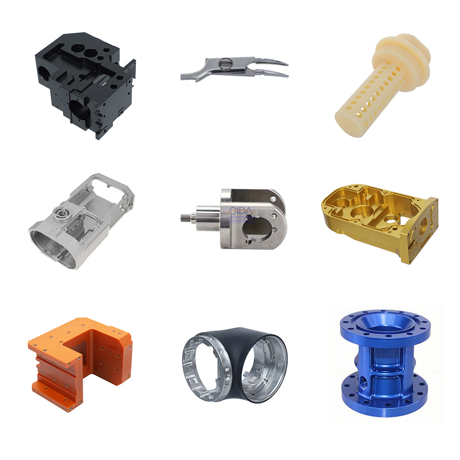


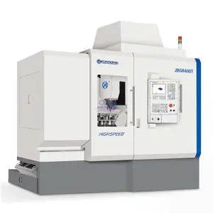
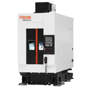
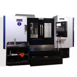
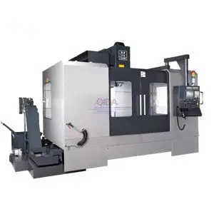
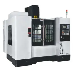
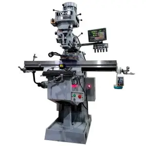
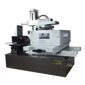
CNC MACHINE
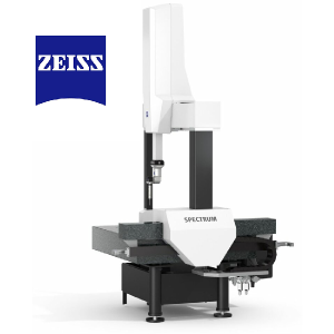
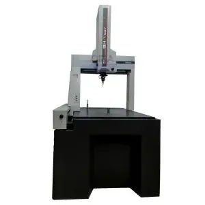
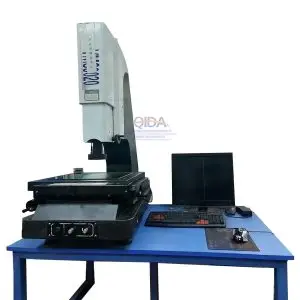
INSPECTION & MEASURING EQUIPMENT
CNC MACHINE
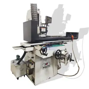
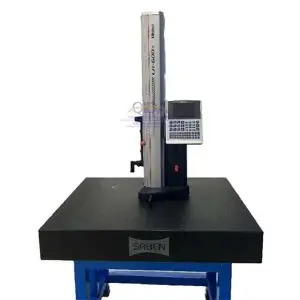
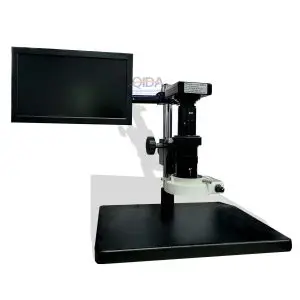
INSPECTION & MEASURING EQUIPMENT
ISO 9001:2015 Certificate
ISO 13485:2016 Certificate
School-Enterprise Coop
Made In China
ISO 9001:2015 Certificate

ISO 13485:2016 Certificate

School-Enterprise Coop

Made In China


